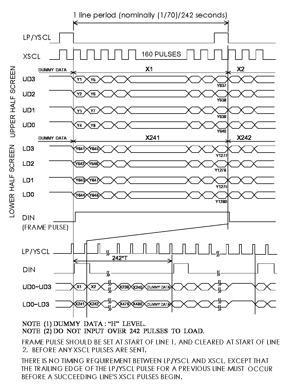
A long time ago I picked up an old LCD module (this one, if its still there). Now the trouble with this module is that it does not have a built in controller. It’s more like a TV or monitor in that it needs to constantly be fed a signal containing the image data to display. Now a standard micro controller might have trouble doing this on its own, it would either require a bit of external circuitry, or have to dedicate the majority of it’s processing time to updating the display. This is a surplus part, and the datasheet provided is poorly xeroxed and lacking specific implementation details. However it is a nice monochrome display at 640×480 and well worth the price of $5.50, if you can get it to work. Luckily for me, I found one other person on the whole internet who managed to get this same display working, and remnants of his work for the MIT Model Railroad club were found here, http://www.nyx.net/~jpurbric/lcd/. Now he managed to implement this using a PIC micro, some discrete logic and some external memories. My plan is to first attempt to drive this from my Papilio board. I had a good start since this other project made really nice timing diagram to follow for the display.
First in implementing the VHDL, I defined as many constant values as I could think up. Using the timing diagram and the datasheet, I setup some time period and count constants.
--Timing Constants
--Time constant integers in nanoseconds
constant CLK_PERIOD : integer := 31; -- approximate/rounded off
constant XSCL_PERIOD : integer := 166 ;

--FRAME CONSTANTS
constant WIDTH : integer := 640;
constant HEIGHT : integer := 480;
constant XPULSES : integer := WIDTH / 4;
constant YPULSES : integer := 242;
The timings I defined at the minimums defined in the datasheet. The nice part about utilizing constants like this, is that I can adjust these later and the whole design should adjust. The CLK_PERIOD constant is the main clock period, so it will be used to keep track of elapsed time. The XSCL_PERIOD is the minimum period of the XSCL pulse or “X Shift Clock”. Looking at the timing diagram it seems that the data is read in on the negative edge of this signal. At first I thought of several other timing constants, but as I worked out the design, they didn’t prove to be necessary. The other constants are pretty obvious, the HEIGHT and WIDTH of the screen in pixels, and the number of YPULSES and XPULSES to be sent in each frame of the signal. If you notice these numbers don’t match up to the size of the display. This display is organized as two screens, an upper and lower half. It’s also 1 bit per pixel. So, of the 8 bit data bus, 4 bits go to the top and 4 go to the bottom. So it only needs to write 160 times for each line to get 640 pixels and it will write 242 lines. Yeah, there are 2 extra lines in the signal but the don’t make it to the display. And now for a couple signals to get started with.
 --Timing signals
signal XSCL_TIME : integer range 0 to (XSCL_PERIOD + CLK_PERIOD) := 0;

--count signals
signal XSCL_CNT : integer range 0 to 160 := 0;
signal YSCL_CNT : integer range 0 to 242 := 0;
The first is my main time delay count. XSCL_TIME will just add on the clock period each time through the main process to make sure we don’t violate our minimum time for the signal. Its defined as a range from zero to XSCL_PERIOD + CLK_PERIOD because I wanted to be sure that whatever size value it ends up being has enough room exceed the XSCL_PERIOD by one clock cycles worth. The XSCL_CNT and YSCL_CNT are regular increment counters to keep track of where we are in the signal and be the main drivers of the state machine.
signal STARTED : STD_LOGIC := '0';
The STARTED signal is just a flag that’s used to have the signal go through as start up process. After the start up, STARTED is set to 1 and stays there.
--Output Signals
signal LP_YSCL : STD_LOGIC := '0';
signal XSCL : STD_LOGIC := '0';
signal UD : STD_LOGIC_VECTOR(3 downto 0) := "0000";
signal LD : STD_LOGIC_VECTOR(3 downto 0) := "0000";
signal DIN : STD_LOGIC := '0';
These are the various output signals, three timing signals and the data signals. For now we will just be sending test pattern on the data. Now for the main process. I think its well commented so I won’t give a line by line explaination. It’s basically a simple state machine, using the current state of the output signals, the XSCL_CNT/YSCL_CNT, and XSCL_TIME signals to track where it is in the process. It follows right along with the timing diagram. Remember that in the process, signals are not updated until after the process.
	--Process Definition
	main: process(clk)
   begin
		-- triggers action on rising edge of clock signal
     if rising_edge(clk) then
	    --increment counter, using time type
		 XSCL_TIME <= XSCL_TIME + CLK_PERIOD;


		 if STARTED='0' then
		   --initial state
			--first part of timing diagram, on LP pulse, and a up/down on XSCL
			if LP_YSCL = '0' then
				--set signals
				LP_YSCL <= '1';
				XSCL <= '1';
				--reset times
				XSCL_TIME <=0;
			elsif LP_YSCL = '1' and
						XSCL = '1' AND
						XSCL_TIME > (XSCL_PERIOD/2) then
				--set signal
				XSCL <= '0';
			elsif LP_YSCL = '1' AND
						XSCL = '0' AND
						XSCL_TIME > XSCL_PERIOD THEN
				--clear started flag
				STARTED <= '1';
				--reset timer
				XSCL_TIME <= 0;
			end if;
		else
			--after started
			if LP_YSCL = '0' and
				XSCL = '0' and
				XSCL_CNT = 0 THEN
				--occurs at the end of a row, timing specs say LP_YSCL must go to zero before XSCL goes high
				--Raise XSCL to HI
				XSCL <= '1';
				--reset pulse timer
				XSCL_TIME <= 0;

				--update X count
				XSCL_CNT <= XSCL_CNT + 1;
			elsif LP_YSCL = '1' and
			--first step, LP is H, XSCL is L, XSCL_CNT is 0
				XSCL = '0' AND
				XSCL_CNT = 0 THEN

				--drop LP, Raise XSCL, load data
				LP_YSCL <= '0';
				XSCL <= '1';

				--temp data
				UD <= "0101";
				LD <= "0101";

				--reset timer
				XSCL_TIME <= 0;

				--if first row, raise frame pulse
				if YSCL_CNT = 0 then
					DIN <= '0';
				end if;
			elsif XSCL = '1' AND
					XSCL_TIME > (XSCL_PERIOD/2) THEN
				--drop xscl to L
				XSCL <= '0';

			elsif XSCL = '0' AND
					XSCL_TIME > XSCL_PERIOD THEN


				--load new data
				--TODO

				--IF at last pulse raise LP to hi
				if XSCL_CNT = XPULSES - 2 then -- use pulses-2 to compensate for cnt not updated yet and zero based index.
					--last X pulse, raise LP
					LP_YSCL <= '1';
					--update X count
					XSCL_CNT <= XSCL_CNT + 1;

					--Raise XSCL to HI
					XSCL <= '1';
					--reset pulse timer
					XSCL_TIME <= 0;

				elsif XSCL_CNT = XPULSES - 1 THEN
				   --new line, drop LP
					LP_YSCL <= '0';
					--reset XSCL_CNT
					XSCL_CNT <= 0;

					if YSCL_CNT = YPULSES - 1 then
						-- this was the last pulse, go back to zero
						YSCL_CNT <= 0;
					else
						--increment Y count
						YSCL_CNT <= YSCL_CNT + 1;
					end if;

				else
					--Raise XSCL to HI
					XSCL <= '1';
					--reset pulse timer
					XSCL_TIME <= 0;
					--update X count
					XSCL_CNT <= XSCL_CNT + 1;
				end if;

			end if;

			--if on first line, first x, raise frame pulse
			if LP_YSCL = '0' AND
				XSCL = '1' AND
				XSCL_CNT = 0 and
				YSCL_CNT = 0 then
				--raise frame pulse
				DIN <= '1';
			elsif LP_YSCL = '0' AND
					XSCL = '1' AND
					XSCL_CNT = 0 AND
					YSCL_CNT = 1 then
				--shut down frame pulse
				DIN <= '0';
			end if;

		 end if; --started

     end if; --clk

   end process;
And the most important part, mapping the signals to the output pin.
	A(0) <= LP_YSCL;
	A(1) <= XSCL;
	A(5 downto 2) <= UD;
	A(9 downto 6) <= LD;
	A(10) <= DIN;
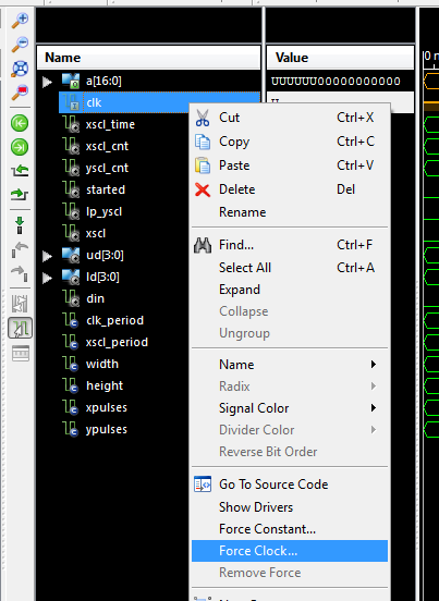
I currently don’t have it setup to connect the display to the FPGA board just yet. I need to wire that up with a 3.3 to 5 logic conversion, since the Spartan3 is a 3.3V part. And looking at the datasheet the minimum “1” voltage is .8*VDD and the minimum VDD is 4.75V. Assuming a 5V supply, I need at least 4V to drive these signals. However, I really should verify the output of this before I go through the trouble of hooking it up anyways. Thankfully, the Xilinx tools come with a simulator that can be used to verify your design.

If you click on your source file in the design explore on the left, select Simulation up top, and the right click on ‘Simulate Behavioral Model’ and select ‘Run’, you should be see the ISim window open up. For me, the first thing I had to do was setup the clock. Oddly, it runs the simulation first with the clock just set as ‘Undefined’. Under the simulation menu, click ‘Restart’ to clear out the current simulation. Right click on the ‘clk’ signal, and select ‘Force Clock’.
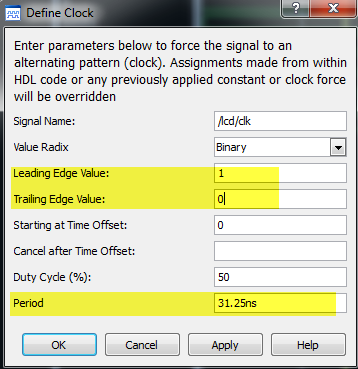
Then you enter the parameters for your clock signal. I really wasn’t sure of the meaning of ‘Leading Edge Value’ and ‘Trailing Edge Value’ so I entered 1 and 0 respectively as they are required fields. Then I just set the clock period of 31.25ns.
Once you’ve done that, can run that for the amount of time you want to see. These commands should be on the toolbar at the top of the window.

Each time you click on the ‘Run for Time Specified’ button, it will add to the simulation, so you can verify the signal a few blocks at a time.

Looks good so far. Hopefully soon I can get it wired up and see if it actually works.
hi! how are you? nice work here…I’m trying to do the same thing as you as I’m affascinated by this lcds, I’ve written a post here http://www.eevblog.com/forum/beginners/how-to-drive-a-old-controllerless-lcd-hitachi-lm236xb/
Would be great if you can read the story (I know its a bit long) and give me some tips…
Thank you very much!
Thanks! I haven’t read through your EEEVBLOG post yet, but I wanted to let you know, the above implementation did work on my LCD. I’m fairly inexperienced with VHDL, so I was only displaying a hardcoded test pattern. I wanted to load images via a serial connection and before posting a follow up to this article. I’ll look at your post when I get a chance, hopefully the controllers are close enough that we can share results. Let me know if you have any questions or sugestions about the article.